
Stackable Mosfet Switch Board (Optical Input)
- Brand: Resonexus
- Product Code: MOS_SW_OPT
- Tariff No: 8537.10.91.20
- Country of Origin: Norway (NO)
- Availability: In Stock
-
€300.00
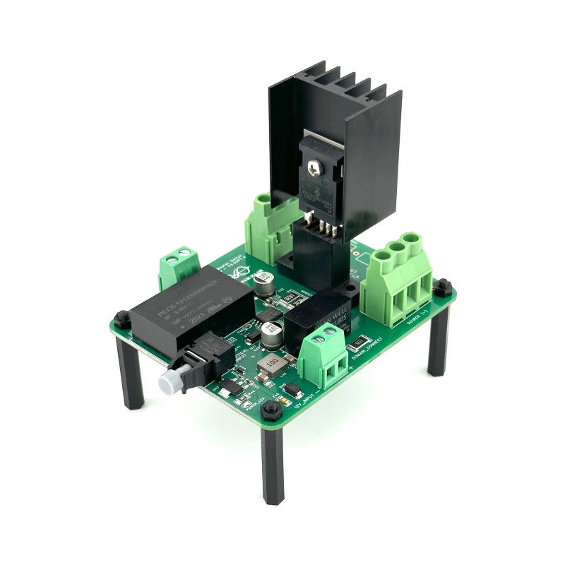
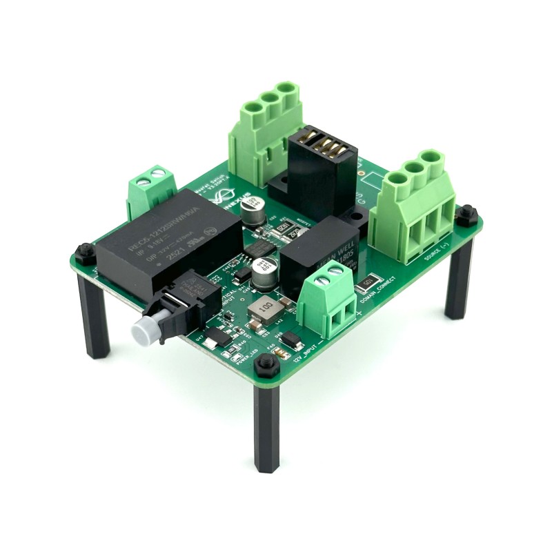
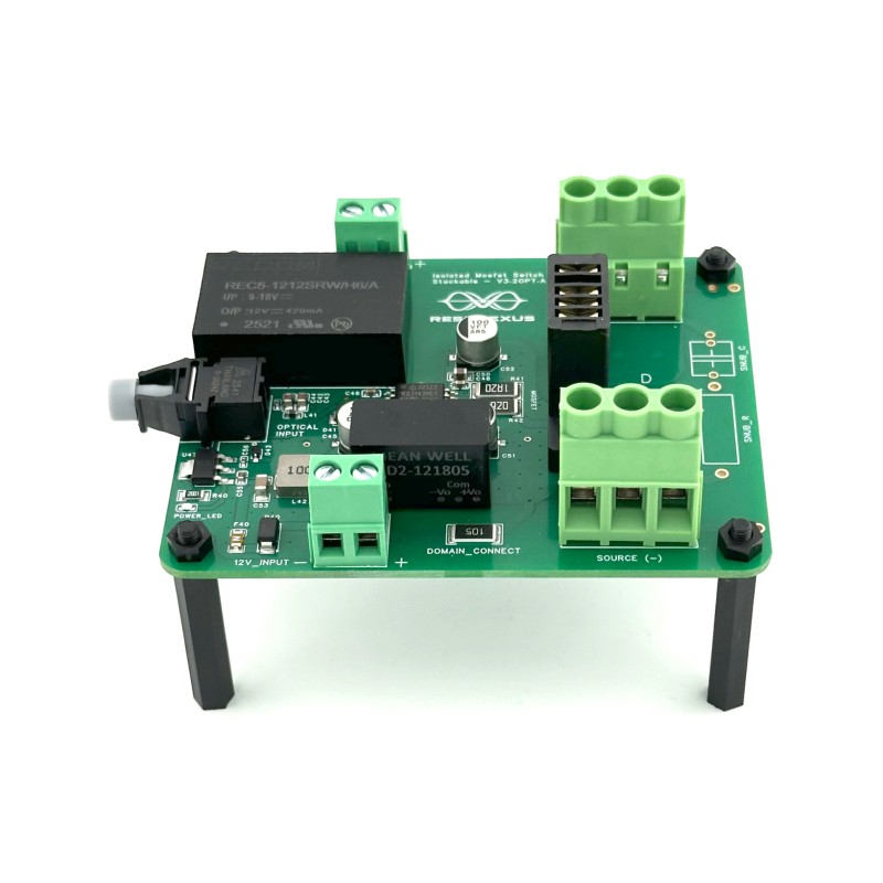
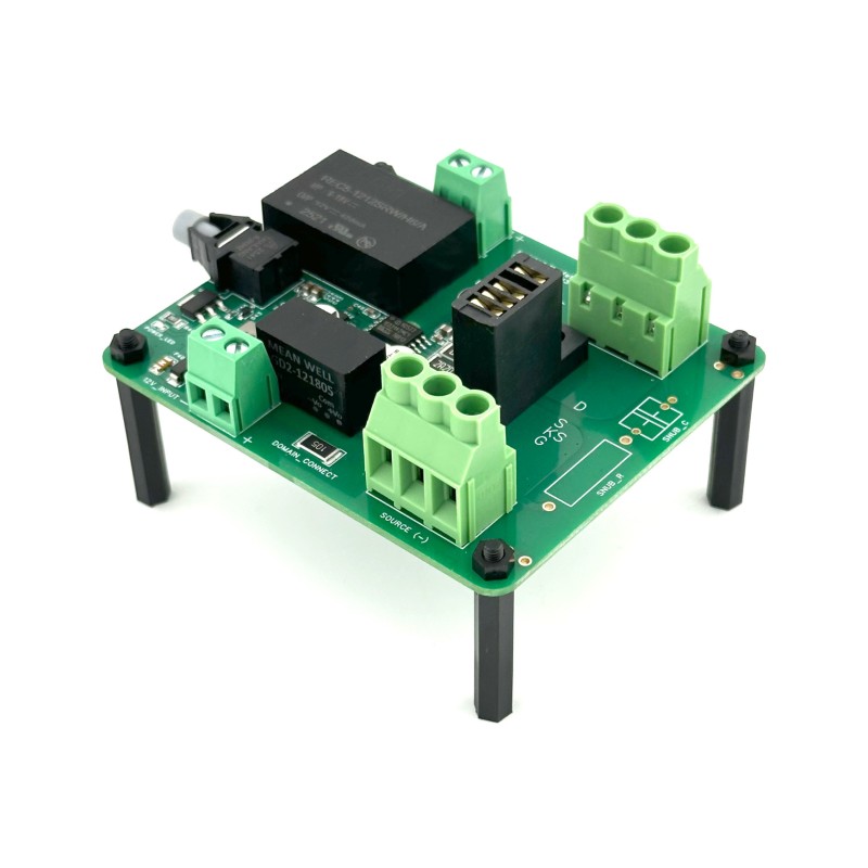
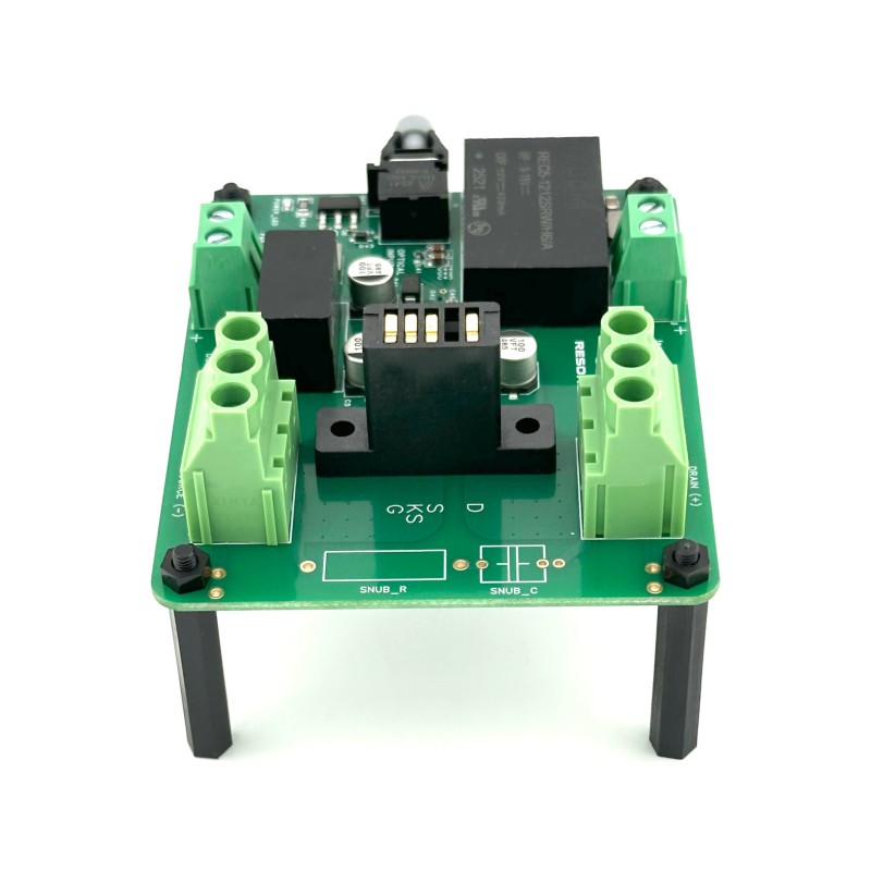
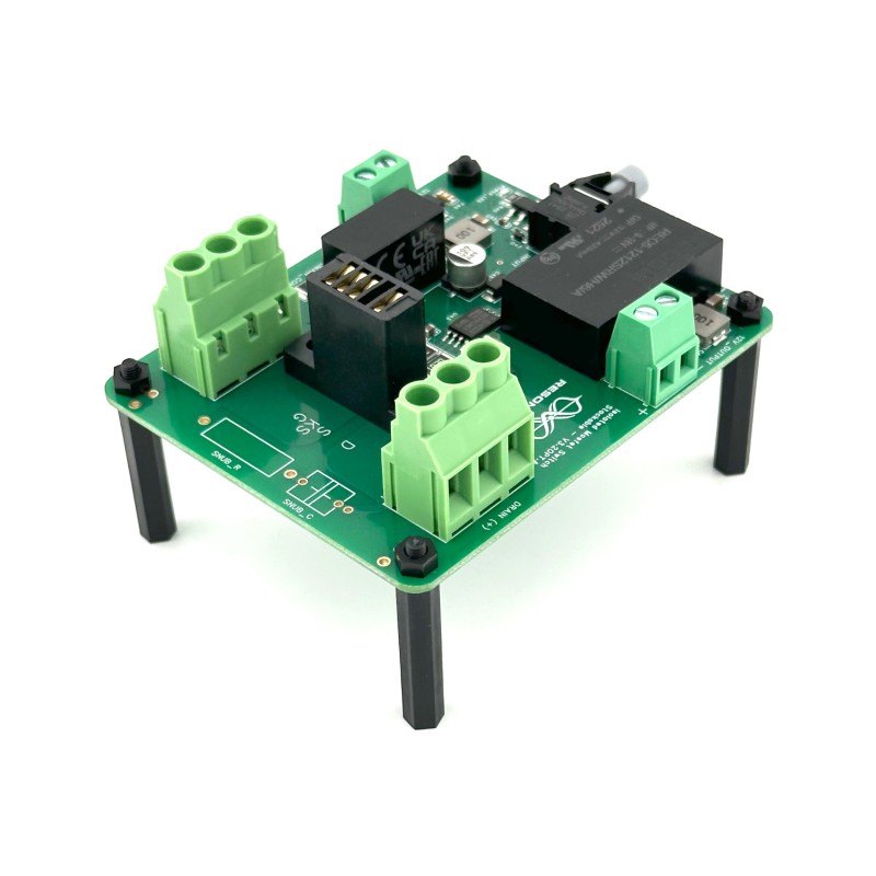
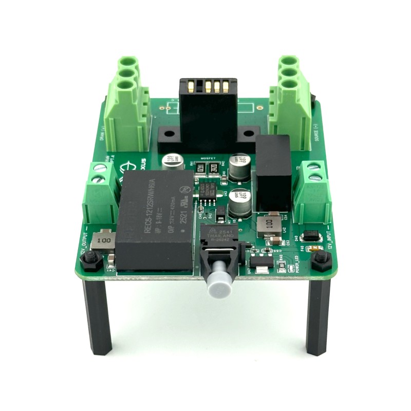
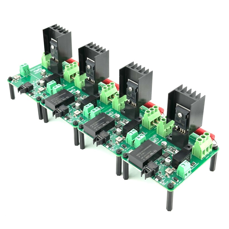
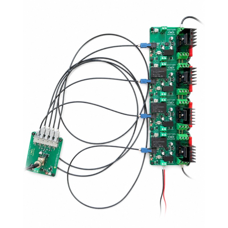
Take high-voltage switching beyond the limits of a single MOSFET with our Stackable MOSFET Switch Board with Optical Input. Designed specifically for series-connected high-voltage MOSFET stacks, each board operates as an independent switching stage with its own isolated gate driver, isolated power domain, fibre-optic signal input, and provisions for DC voltage grading and optional RC snubbing. In the current system architecture, up to five MOSFET switch boards can be connected in series and triggered simultaneously, allowing the voltage capability of the complete switch to scale with the number and voltage rating of the MOSFET stages.
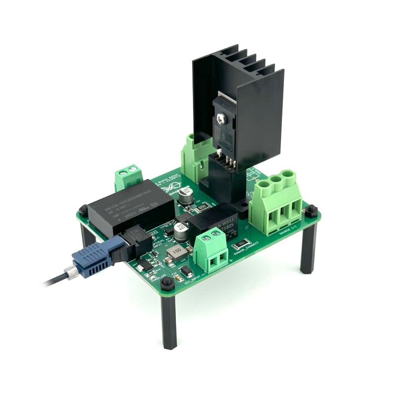
The board is based on the same ultra-fast gate-drive architecture used in our TO-247-4 MOSFET Switch Board, but has been redesigned specifically for synchronized stacked operation. Instead of receiving a BNC signal directly, each stage receives its switching command through a non-conductive fibre-optic connection from our Signal-to-Optical Bridge. This allows MOSFET stages operating at very different electrical potentials to receive closely synchronized switching commands while maintaining galvanic isolation between the low-voltage control electronics and the high-voltage stages.
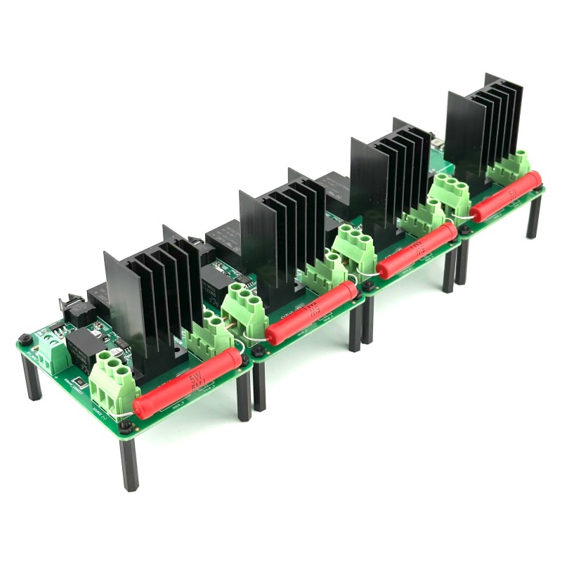
- Stackable from 1 to 5 Stages: Connect up to five boards in series to create a single high-voltage solid-state switch. Each board forms one independently driven MOSFET stage. Five stages is the maximum supported stack size in the current architecture.
- Ultra-Fast Switching: The high-performance isolated gate-driver architecture provides nanosecond-scale switching performance. Actual rise and fall times depend on the selected MOSFET, stack size, load, wiring, grading network, and circuit conditions.
- Fibre-Optic Trigger Input: Each switching stage receives its control signal through optical fibre. The non-conductive connection allows each MOSFET stage to float at its own high-voltage potential.
- Synchronized Multi-Stage Switching: Our Signal-to-Optical Bridge distributes the control signal to up to five synchronized optical outputs. One optical output is connected to each MOSFET switch board. Equal-length fibre cables should be used to minimize timing differences between stages.
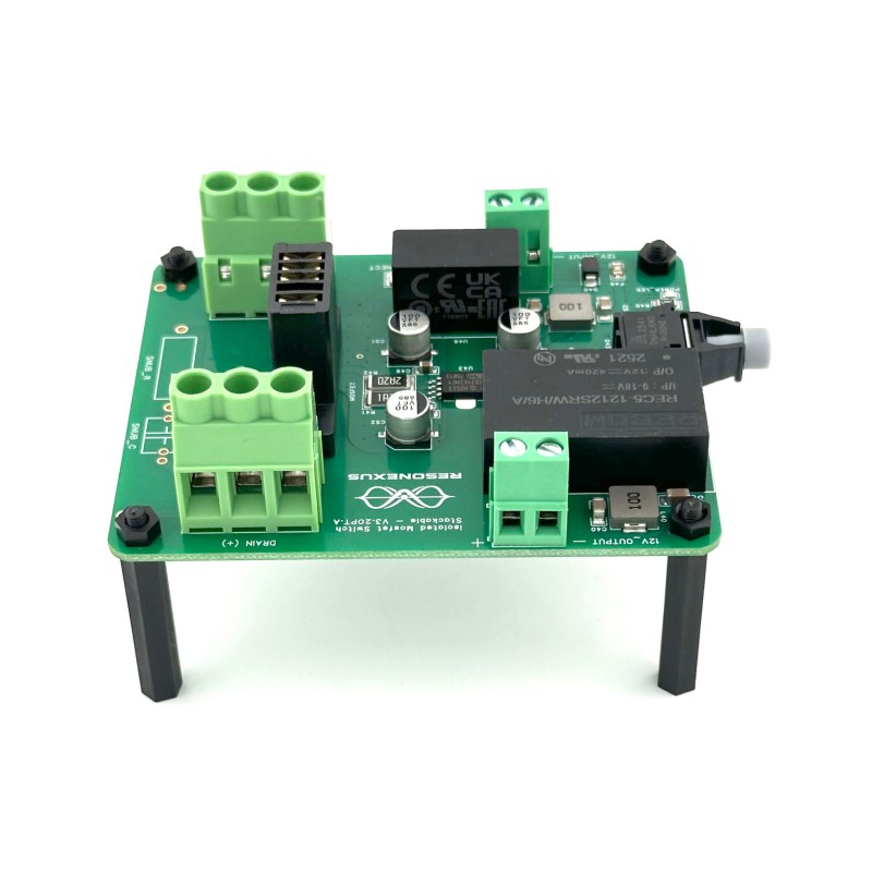
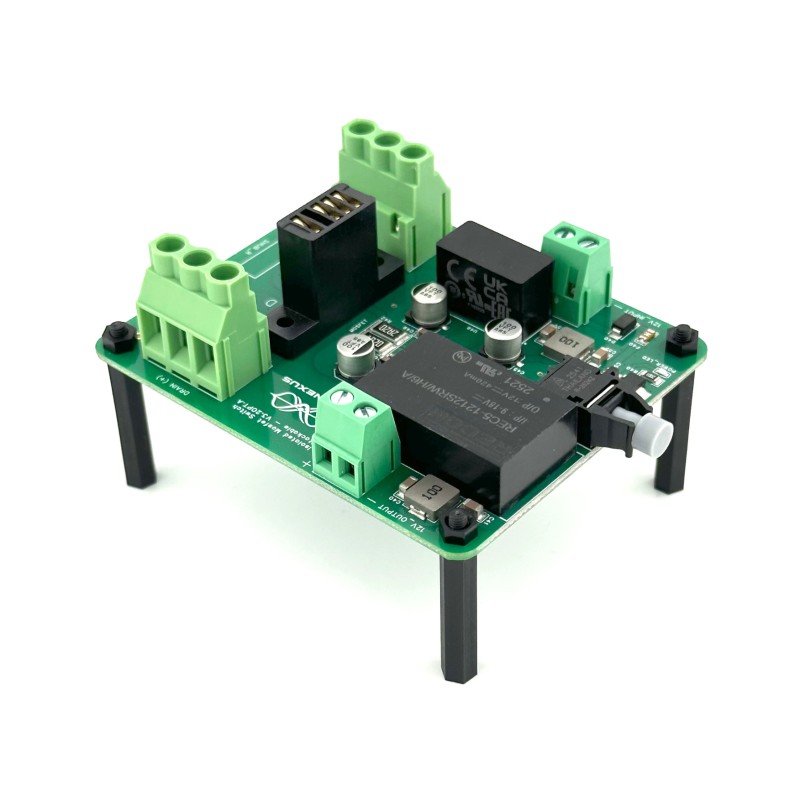
- Cascaded Isolated 12 V Power: Only the first board requires an external 12 V connection. Each intermediate stage contains an isolated DC-DC converter that provides isolated 12 V power to the next board in the chain.
- Independent Isolated Gate Drive: Every stage contains its own isolated gate-driver IC and dedicated isolated gate-drive DC-DC converter, allowing the MOSFET to be driven locally at the electrical potential of its own stage.
- TO-247-4 / TO-247-4L Socket: MOSFETs plug directly into the low-inductance four-lead socket without soldering. The dedicated Kelvin source connection provides a low-inductance reference for the gate driver.
- Required DC Voltage Grading: Each stage must have a suitable high-voltage grading resistor connected across drain and source for stacked operation. Together, these resistors form a controlled resistive divider that helps distribute the total OFF-state voltage evenly between the MOSFETs.
- Flexible Grading Resistor Installation: The grading resistor can either be soldered into the dedicated PCB mounting points or connected directly across the drain and source screw terminals.
- Optional RC Snubber Support: Dedicated PCB pads are provided for a series RC snubber across each stage. A properly selected snubber can help reduce ringing, voltage overshoot, and high-frequency oscillation.
- High-Side or Low-Side Switching: The optical architecture supports both low-side and high-side configurations. For high-side operation, we strongly recommend powering the stack from a floating 12 V battery.
- High-Frequency Performance: Switching frequencies above 1 MHz are possible under suitable conditions. The practical limit depends on MOSFET gate charge, number of stages, duty cycle, temperature, and isolated DC-DC loading.
- Fast Pulse Generation: A minimum input pulse width of 50 ns is recommended for general stacked operation to ensure that all stages switch fully and synchronously.
- Built-In Fuse Protection: Onboard fuse protection provides additional protection for the auxiliary power circuitry.
- High-Current Screw Terminals: Robust drain and source screw terminals provide the electrical connection between stages and to the external high-voltage circuit.
Why Use Series-Connected MOSFETs?
By connecting multiple MOSFET stages in series, the applied voltage can be distributed across several devices. With the maximum five-stage configuration, five 3300 V MOSFETs have a theoretical combined blocking capability of 16.5 kV.
A safety margin is required for switching transients, timing mismatch, parasitic inductance, ringing, and imperfect voltage sharing. We recommend maintaining approximately 10% voltage margin below the theoretical stack rating. A five-stage stack using 3300 V MOSFETs therefore has a recommended operating voltage of approximately 14.85 kV, conveniently considered approximately 15 kV, unless the specific configuration has been separately validated for higher voltage.
Static and Dynamic Voltage Sharing
Reliable series MOSFET operation requires both good static and dynamic voltage sharing. Leakage-current differences and other parasitic leakage paths can otherwise cause the OFF-state voltage to distribute unevenly. DC grading resistors provide a defined current path across every stage and help distribute the total DC voltage evenly.
During switching, differences in gate threshold voltage, gate charge, capacitance, propagation delay, and switching speed can cause one MOSFET to turn on or off slightly earlier than another. A slower device may then temporarily block a disproportionately large part of the total stack voltage. Synchronized optical triggering and matched MOSFET characteristics are therefore particularly important at high voltage and high switching speed.
MOSFET Matching and Timing Verification
Properly matched MOSFETs are an important requirement for reliable stacked operation. Differences in gate threshold voltage, gate capacitance, gate charge, and switching characteristics can cause individual MOSFETs to turn on or off at slightly different times. In a series-connected stack, this timing mismatch can temporarily force one device to block a disproportionately large share of the total stack voltage during a switching transition.
For this reason, customers purchasing multiple boards for a new stacked configuration should select our MOSFET Matching and Timing Verification option. When selected, we carefully measure and select MOSFETs with closely matched electrical properties and verify the switching behavior of the set. The MOSFETs are treated as a matched group for the ordered stack rather than as unrelated individual devices, helping reduce stage-to-stage timing variation and improve dynamic voltage sharing.
The matching service is shown as an optional product selection only because some users may already have a suitable set of matched and verified MOSFETs. If you are purchasing MOSFETs from us for a new multi-board stack, the MOSFET Matching and Timing Verification option should be selected. Users supplying their own MOSFETs are responsible for ensuring that the devices are sufficiently matched for series-stacked operation.
Signal-to-Optical Bridge
Our Signal-to-Optical Bridge is required for synchronized stacked operation and is available separately. It accepts a conventional electrical control signal through BNC and converts it into up to five synchronized optical outputs. The bridge accepts both 3.3 V and 5 V logic-level square waves and can be driven from a function generator, pulse generator, MCU, or other suitable source.
Fibre Optic Cable
Each MOSFET switch board requires a compatible fibre-optic cable to connect it to the Signal-to-Optical Bridge. The cable is therefore required for every stage during normal stacked operation. It is offered as an optional product selection only because users may already own suitable compatible fibre-optic cables. All cables in a stack should have the same length to minimize propagation-delay differences.
DC Grading Resistor
Each stage requires a suitable high-voltage DC grading resistor connected in parallel with the MOSFET drain-source terminals. The resistor is offered as an optional product selection because users may already have suitable high-voltage resistors. This does not mean the grading resistor itself is optional for stacked operation.
Lower-value grading resistors provide stronger voltage balancing but increase continuous power dissipation. Higher resistance values reduce standby losses but provide weaker balancing. As an example, five 10 MΩ grading resistors create a total grading resistance of 50 MΩ. With 15 kV across the five-stage stack, approximately 300 µA flows through the grading network. Each resistor drops approximately 3 kV and dissipates approximately 0.9 W. If you are unsure which resistor value to choose, we recommend 10 MΩ per stage as a good starting point.
RC Snubber Kit
The optional RC Snubber Kit includes a 120 Ω high-voltage resistor and a selection of high-voltage, high-frequency capacitors from 5 pF to 47 pF. Unlike the fibre-optic cables and DC grading resistors, the RC snubber is not required for normal operation. It is intended for setups where measurements indicate excessive ringing, voltage overshoot, or undesirable dynamic voltage sharing.
High-Voltage Pulse Capacitors
For pulsed-power and capacitor-discharge applications, we also offer high-voltage pulse capacitors that can be used together with the MOSFET switch stack. These capacitors are suitable for storing the energy required for fast high-voltage pulse experiments and can be combined with the stack as part of a complete switching setup. When switching or discharging a pulse capacitor, a suitable series ballast resistor must be used to limit the peak discharge current through the MOSFET stack. Without sufficient series resistance, the instantaneous current can become extremely high and may exceed the maximum pulsed-current rating of the MOSFETs, potentially damaging the devices. The ballast resistance should therefore be selected so that the maximum expected peak current remains within the pulsed-current rating of the MOSFETs used in the stack. Suitable high-voltage pulse capacitors and 50 W non-inductive resistors for use as ballast resistors can be found in the Related Products section below.
TO-247-4 / TO-247-4L Package Support
The board supports compatible TO-247-4 and TO-247-4L MOSFETs. The dedicated Kelvin source pin provides the gate driver with a low-inductance source reference separate from the main load-current path, reducing common-source inductance and improving gate signal integrity during high di/dt switching.
Typical Applications:
- Nanosecond and sub-microsecond high-voltage pulse generation
- Pulsed-power experiments
- High-voltage capacitor discharge control
- Spark-gap triggering and ignition systems
- Plasma and electrical discharge experiments
- Inductive pulse systems
- Resonant and high-frequency high-voltage experiments
- Research requiring switching voltages beyond the capability of a single MOSFET
Measured Switching Performance
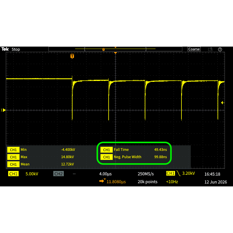
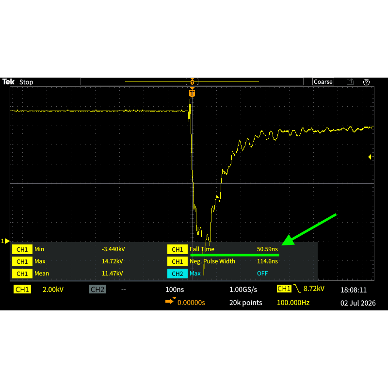
A complete five-stage stack has been measured with approximately 50 ns rise and fall times. These measurements were made using a 10 MHz-bandwidth high-voltage probe, which significantly limits the observable edge speed. The actual MOSFET switching transitions may therefore be considerably faster than the displayed 50 ns measurement. A separate oscilloscope screen capture showing the measured five-stage stack waveform is included among the product images.
Typical propagation delay from the electrical signal input on the Signal-to-Optical Bridge to the MOSFET gate is approximately 85 ns. Typical maximum pulse-width distortion from the bridge input to the resulting MOSFET switching signal is approximately 7 ns. When the MOSFET Matching and Timing Verification service is selected, we guarantee a switching skew/mismatch of less than 2 ns between the matched MOSFET stages.
Technical Specification:
| Board Supply Voltage | 12 V DC |
| Control Input | Fibre Optic |
| Optical Connection Type | Versatile Link, 1 mm POF |
| Optical Wavelength | 650 nm |
| Output Gate Voltage (Vgs) | -5 V / +18 V |
| Max Load Current | 20 A |
| Gate Driver Isolation Rating | 2300 V DC / 5600 V transient |
| Inter-Stage Power Transfer | Isolated 12 V DC-DC |
| Supported Device Package | TO-247-4 / TO-247-4L |
| Supported Stack Size | 1–5 MOSFET Switch Boards |
| Minimum Pulse Width | 27 ns (single stage) / 50 ns (stacked) |
| Switching Frequency | >1 MHz possible, configuration-dependent |
| Measured Rise Time, 5-Stage Stack | Approx. 50 ns* |
| Measured Fall Time, 5-Stage Stack | Approx. 50 ns* |
| Input-to-Gate Propagation Delay | Typ. 85 ns |
| Maximum Pulse-Width Distortion | Typ. 7 ns max |
*Rise and fall time were measured on a complete five-device stack using a 10 MHz-bandwidth high-voltage probe. The limited probe bandwidth restricts the measured edge speed, so the actual switching transitions may be significantly faster than approximately 50 ns. See the separate oscilloscope screen capture in the product images.
Datasheets for selectable MOSFETs can be found here: GP3T080A120H — MSC080SMB120B4N — MSC035SMA170B4 — MSC400SMA330B4N — MSC080SMA330B4N
Required Components for Stacked Operation
A complete multi-stage switch requires one compatible fibre-optic cable and one suitable DC grading resistor for every MOSFET switch board, together with a Signal-to-Optical Bridge providing one synchronized optical output for each stage. The fibre cables and grading resistors are selectable extras because users may already own suitable components; their absence from an order does not mean they can be omitted from the operating circuit. Likewise, the MOSFET Matching and Timing Verification service should be selected when purchasing MOSFETs for a new stacked configuration unless the user already has a suitably matched and verified set of MOSFETs.
Important: The practical maximum voltage, current, switching frequency, pulse width, and switching speed depend on the MOSFET type, number of stages, load, wiring inductance, duty cycle, cooling, grading network, snubber configuration, and overall circuit design. Always begin testing at a voltage below the rating of a single MOSFET and verify correct operation of every stage before increasing the stack voltage.
For high-voltage stacked operation, MOSFET matching, equal-length fibre-optic cables, correctly selected DC grading resistors, stable 12 V power, and proper high-voltage measurement practices are essential. Please refer to the supplied instruction manual before assembling or operating a multi-stage switch.
The Stackable MOSFET Switch Board with Optical Input provides a flexible platform for building extremely fast solid-state switches at voltages far beyond the capability of a single semiconductor device. By combining isolated gate drive, fibre-optic synchronization, cascaded isolated power, configurable DC grading, and optional dynamic snubbing, the system provides researchers and advanced experimenters with a powerful platform for high-voltage pulsed-power and high-speed switching applications.
This product includes a heatsink suitable for TO-247-sized MOSFETs. If additional heatsinks are required for other MOSFETs or applications, they can be selected as an optional extra.
| Technical | |
| Input voltage | 12 V |
| Input signal | Optical (fibre optic) |
| Max DC isolation voltage | 2300 V |
| Max transient isolation voltage | 5600 V |
| Max frequency | > 1 MHz |
| Output gate voltage (Vgs) | -5 / 18 V |
| Rise time | Typ. 15 ns (single stage) |
| Fall time | Typ. 15 ns (single stage) |
| Minimum input pulse width | 27 ns (single stage) / 50 ns (stacked) |
| Input to output propagation delay | 85 ns |
| Max load current | 20 A |
| Supported device package | TO-247-4 / TO-247-4L |
Related Products
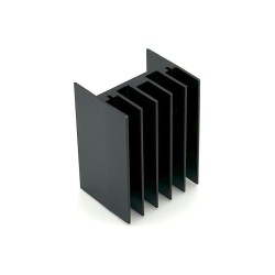
Heatsink for TO-247 package
Upgrade your cooling setup with our high-performance heatsink, specifically designed for the TO247 p..
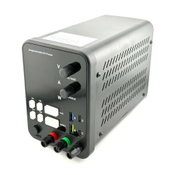
Variable Power Supply DC (120V - 3A) with Memory Function
Our Variable DC Power Supply with Memory Function is engineered with cutting-edge technology to deli..
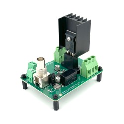
Mosfet Switch Board (TO-247-4)
Unlock next-generation versatility and extreme switching performance with our redesigned MOSFET Swit..
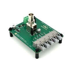
Signal to Optical Bridge
Convert a standard low-voltage control signal into multiple synchronized fibre-optic trigger signals..
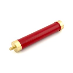
High Voltage Resistor (30kV, 50W, 1kΩ–100kΩ)
Designed for demanding high-voltage circuits requiring controlled current limiting, pulse-energy han..
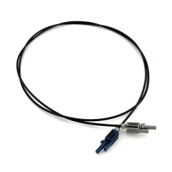
Fibre Optic Cable (1m)
This 1m fiber optic cable is intended for reliable signal transmission between our Signal to Optical..
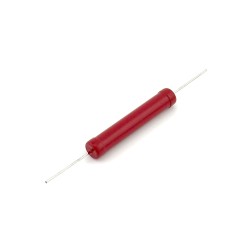
High Voltage Resistor (25kV, 5W, 100kΩ–10MΩ)
Designed for compact high-voltage circuits requiring accurate resistance, controlled current flow, a..
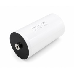
High Voltage Pulse Capacitor (20kV - 220nF - 100A)
Our 20 kV high voltage pulse capacitor is designed for demanding pulsed-power, high-voltage switchin..