
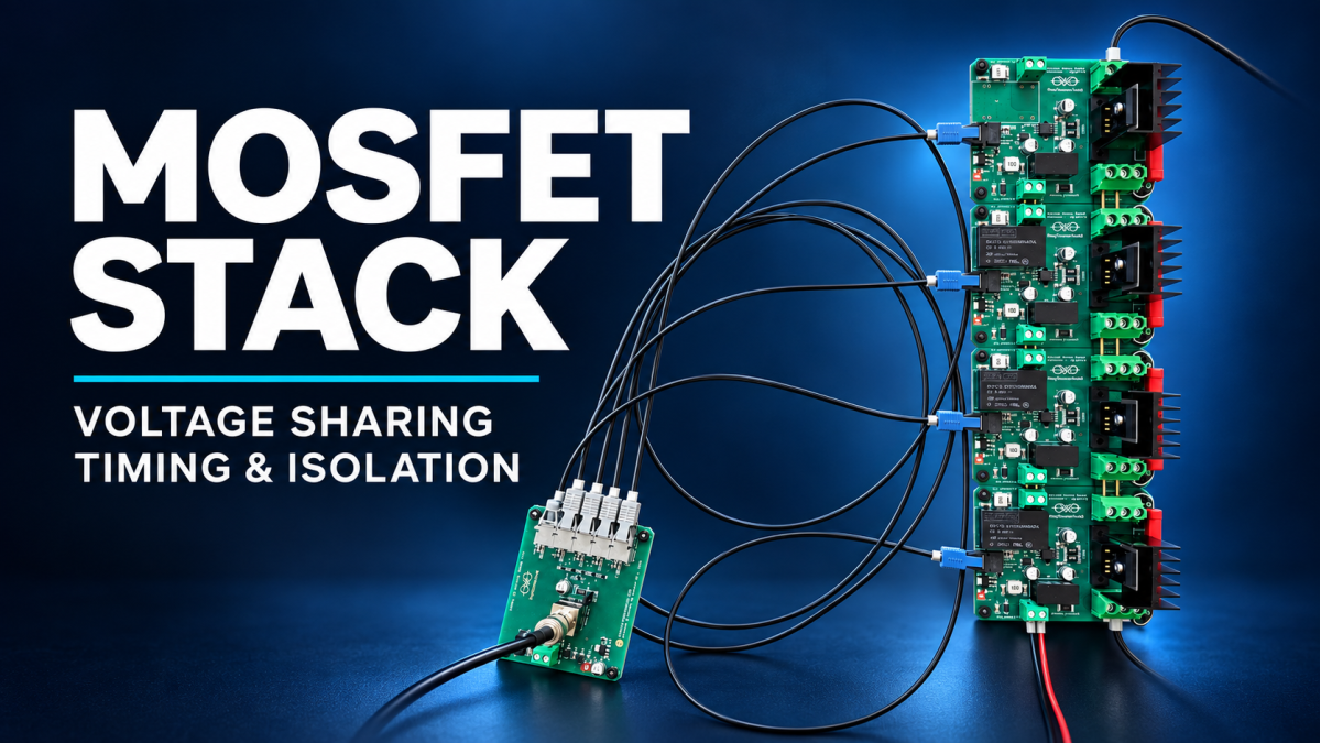
A mosfet stack connects several MOSFETs in series so they can act as one switch at a voltage beyond the rating of an individual device. The difficult part is making every stage share the voltage, including during transitions that last only tens of nanoseconds. Equal device ratings and a common trigger command do not automatically produce equal electrical stress.
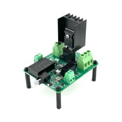
Our Stackable MOSFET Switch Board with Optical Input brings the main building blocks together: local gate drive, optical triggering, cascaded auxiliary power, DC grading and optional snubber connections. This guide explains the problems each feature addresses, how to estimate the important limits and what still needs checking in the assembled circuit.
In this guide: Series operation · Our stack architecture · DC voltage balancing · Switching timing · Gate drive and isolation · 12 V power · Voltage and current limits · Verification · Q&A
What is a MOSFET stack, and why connect MOSFETs in series?
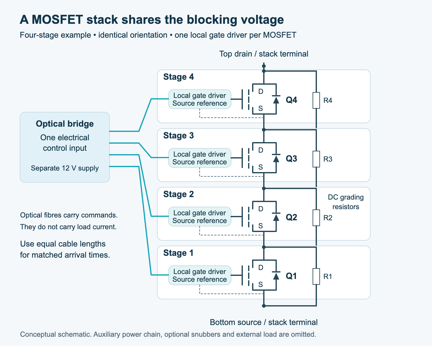
In a series stack, the source of one MOSFET connects to the drain of the next. The same load current passes through every stage. When all devices are on, their on-state voltage drops add. When they are off, the total voltage must divide across the individual drain–source terminals.
For N identical stages with ideal voltage sharing:
Vstage = Vstack / N
RDS(on),stack ≈ N × RDS(on),device
Four stages blocking 10 kV would therefore each support approximately 2.5 kV. Stacking raises the possible blocking voltage; it does not multiply the current rating. The extra on-resistance and switching losses also need cooling.
A same-direction series stack is different from a back-to-back MOSFET switch. Back-to-back devices oppose their body diodes to block either polarity. The stack discussed here uses the same MOSFET orientation throughout and does not provide bidirectional off-state blocking. Applications include high-voltage pulse generation, capacitor-discharge control and controlled electrical-discharge experiments.
How our stackable MOSFET switch is arranged
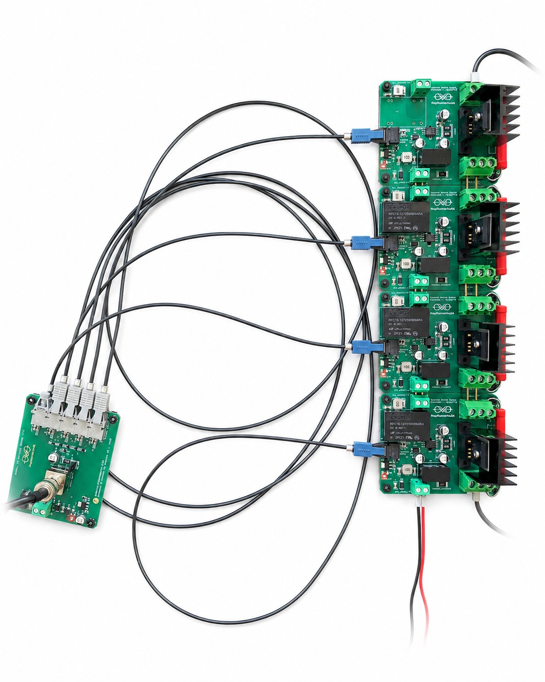
The current system supports one to five boards. Each board holds one compatible TO-247-4 or TO-247-4L MOSFET and its local drive circuitry. Copper conductors join adjacent drain/source terminals; the external switch terminals are the bottom board’s source and the top board’s drain.
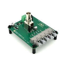
A separate Signal to Optical Bridge distributes one BNC control input to up to five optical outputs. Each stage receives its own fibre. The bridge has a separate 12 V supply, while the stack receives external 12 V power at its bottom board and forwards isolated power up the chain.
For a supplied and verified set, keep the boards in their marked order. This preserves the arrangement used during testing, including its interconnections and parasitic layout. When buying a new stack with MOSFETs from us, select MOSFET Matching and Timing Verification. The fibre, grading-resistor and matching selections are separate purchasing options because some users already own suitable parts; they are not reasons to omit those functions.
Static voltage balancing: why every stage needs a grading resistor
Off-state MOSFETs have leakage current, and that leakage varies with device, temperature and applied voltage. PCB contamination and other leakage paths add uncertainty. Without deliberate grading, the lowest-leakage stage can take too much of the total blocking voltage.
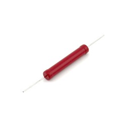
We address this with a high-voltage resistor across the drain and source of every stage. The resistor network establishes a predictable DC current path. Use the same resistance on all stages and tight tolerances; our selectable grading resistors are specified at 1%. A larger grading current makes leakage differences less influential, but increases continuous dissipation.
For equal resistors RG and approximately equal voltage sharing:
Igrading ≈ Vstack / (N × RG)
Presistor ≈ (Vstack / N)2 / RG
| Resistance per stage | Grading current | Power per resistor | Total grading power |
|---|---|---|---|
| 10 MΩ | 250 µA | 0.625 W | 2.50 W |
| 6.8 MΩ | 368 µA | 0.919 W | 3.68 W |
| 4.7 MΩ | 532 µA | 1.33 W | 5.32 W |
These nominal calculations assume equal sharing and negligible extra leakage. Our manual uses 10 MΩ per stage as a practical starting point, not a universal selection rule. Verify resistor working voltage, power derating, tolerance, spacing and leakage at the intended temperature. Our 25 kV, 5 W high-voltage resistors include the relevant resistance values; the voltage and wattage limits must both be respected. The high-voltage resistor divider guide explains why those are separate constraints.
Dynamic voltage sharing: nanoseconds matter
DC grading controls the settled off-state voltage. It cannot guarantee voltage balance during a fast switching edge. At turn-on, a late-switching MOSFET can remain blocking while the other stages conduct. At turn-off, an early-switching MOSFET can begin supporting voltage while the others are still on. Both cases can overstress a stage despite acceptable total stack voltage.
We reduce these differences with matched MOSFET characteristics, a common optical bridge, equal-length fibres and consistent local gate-drive hardware. Keep the matched devices together: replacing one with another of the same voltage rating is not sufficient evidence of matching. Threshold voltage, gate charge, capacitance and actual switching behaviour matter.
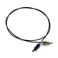
Our 1 m fibre-optic cable has a typical propagation delay of 5 ns/m. A one-metre length difference would therefore introduce about 5 ns of additional arrival-time difference before receiver and MOSFET variations are considered. Use equal lengths, secure the latching connectors and avoid tight bends.
The current product specification gives less than 2 ns switching skew for stages supplied with our Matching and Timing Verification service. That specification belongs to the matched, verified set; changing devices, power conditions or the installation still requires checking the result. Matching and optical synchronization reduce causes of imbalance. They do not amount to active closed-loop regulation of every stage voltage.
Local gate drive, Kelvin source and common-mode transients
Each gate must be driven relative to its own source, which may be thousands of volts away from ground. Connecting all gates to one ground-referenced driver would not maintain the correct gate–source voltage. Our board provides a local gate driver and dedicated isolated gate-drive supply for each MOSFET.
The four-lead socket includes a Kelvin source connection: the driver return is separate from the main load-current source connection. This reduces the voltage disturbance coupled into the gate loop by rapidly changing load current. It helps preserve the intended gate waveform; short, well-arranged external power wiring remains important.
Our drive levels are approximately −5 V off and +18 V on. Negative off-state bias helps resist unwanted turn-on, but a replacement MOSFET must tolerate both levels with margin. Never assume every TO-247-4 device has compatible pin assignments or gate-voltage limits.
Fast voltage movement also tests common-mode transient immunity (CMTI). This describes a driver’s ability to keep functioning while the voltage between its reference domains changes rapidly. A DC isolation-voltage rating and a CMTI rating describe different stresses. Optical control removes a conductive signal path to the bridge; it does not remove all capacitive coupling or interference around the switching hardware. See TI’s explanation of CMTI for the distinction.
The 1 MΩ DOMAIN_CONNECT resistor is not the grading resistor
Each board also contains a 1 MΩ DOMAIN_CONNECT resistor. It references the local signal/power domain to the MOSFET-side domain so the two do not drift to excessively different DC potentials. It is a physical electrical connection, despite its high resistance. It must remain installed on every board used in a stack.
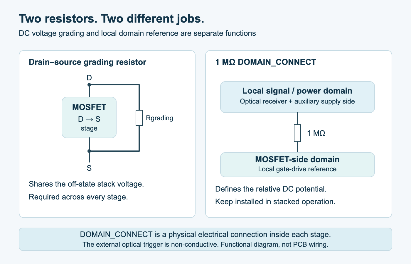
The manual permits removing DOMAIN_CONNECT only for particular standalone applications. That does not increase the specified internal isolation limits of 2,300 V DC or 5,600 V transient. For stacked operation, leave it fitted.
Why the 12 V power chain can limit a MOSFET stack
Only the bottom board receives external 12 V power. Intermediate boards forward isolated 12 V power to the next stage. This avoids running a separate external power lead to every floating board, but it creates a cumulative load: upstream converters must support the stages beyond them as well as the conversion losses.
The PS_EN jumper controls the outgoing 12 V supply. Leave it enabled on boards that feed another stage; disable it on the last board. Disable it for standalone operation too. This removes unnecessary converter consumption. It does not replace DOMAIN_CONNECT or change the grading network.
Gate-drive energy demand rises with switching frequency and MOSFET gate charge. If the supply chain sags, upper stages can lose proper drive while lower stages continue switching. A flashing or lit LED is not a substitute for verifying the supply voltage under the intended switching conditions.
For high-side operation, our manual recommends a floating 12 V battery. An ordinary bench supply with apparently floating outputs may have an output-to-earth rating far below the common-mode voltage imposed by the circuit. A battery removes that bench-supply path, but the battery, wiring and entire assembly still require suitable insulation and clearance from earth. Keep the battery charged and low-voltage instruments physically separated from the high-voltage discharge area.
Optional RC snubbers: damping comes with a cost
Parasitic inductance and capacitance can produce ringing and overshoot. Each board includes pads for a series RC snubber across the stage, providing a practical way to add damping when measurements show it is needed.
A snubber changes the switching transient and dissipates energy. Larger capacitance can reduce edge speed and increase losses, especially at high repetition rates. Choose components for the actual waveform, pulse voltage and dissipation; installing the same arbitrary capacitor everywhere does not prove dynamic balance. Our optional snubber kit supports experimentation, while the assembled circuit determines the final choice.
Microchip’s AN6507 on series-connected SiC MOSFETs discusses passive balancing and probe-induced imbalance. Its RCD topology includes a diode and differs from our board’s optional series RC network; component values and results should not be transferred directly.
Voltage, current and heat: three different limits
Do not use the sum of the MOSFET ratings as the operating voltage
Four 3,300 V MOSFETs have a theoretical rating sum of 13.2 kV. The supplied manual recommends at least 20% voltage margin, giving 13.2 kV × 0.8 = 10.56 kV, rounded to approximately 10.5 kV in its example.
Use that as a conservative design starting point for the manual’s four-stage example. Every stage must still stay below its limit during switching and ringing, with sufficient board insulation and external clearances. Confirm the applicable limits for the exact MOSFETs and assembled stack; changing stage count is not just an arithmetic upgrade.
Every stage carries the full load current
The board’s listed maximum load current is 20 A, but MOSFET current capability, pulse duration, safe operating area, connector limits and cooling can impose a lower limit. More stages do not turn a 20 A current path into an 80 A path.
For approximately constant hot on-resistance, conduction heating is Pcond ≈ IRMS2 × ΣRDS(on). Switching losses and snubber losses add to it. Use resistance at operating temperature and the actual RMS current, not just a short pulse’s average current.
In capacitor-discharge circuits, stored energy is E = ½CV². A supply’s current limit does not limit the instantaneous discharge current from a charged capacitor. The manual therefore requires series ballast resistance. As an initial resistive estimate, Ipeak ≈ Vcapacitor/Rtotal; account separately for the real load, inductance and transient waveform.
Our 30 kV, 50 W non-inductive resistor is a relevant ballast option. Its 50 W rating is not a pulse-energy allowance: check pulse duration, joules per event, repetition rate and voltage as well. A spark-gap bleed resistor serves another purpose—setting the gap’s off-state potential—and must withstand the brief voltage pulse before the gap conducts.
How fast can the stack switch?
The current product page reports approximately 50 ns rise and fall times on a five-stage stack measured with a 10 MHz high-voltage probe. The probe limits observable edge speed, so this is a measurement under stated conditions, not a universal intrinsic switching time. The separate typical 15 ns single-stage figure must not be presented as a guaranteed five-stage result.
Propagation delay is different again: the listed typical delay from the optical bridge’s electrical input to the MOSFET gate is approximately 85 ns, with typical pulse-width distortion around 7 ns. An edge can be fast after a longer, repeatable delay. For normal stacked operation, keep input pulses at least 50 ns wide.
Operation above 1 MHz is possible in suitable configurations, but it is not a promise of maximum voltage and current at that frequency. The manual’s auxiliary-power test checks the installed stack without high voltage: increase frequency, verify stable 12 V output, allow at least five minutes for thermal effects and retain at least 20% margin below the highest stable result. This establishes a power-chain limit, not the high-voltage switching-loss or load limit.
Verify each stage, not just the total output pulse
High-voltage switching involves lethal voltage and stored energy. Assemble and alter the circuit only after isolation, discharge and verification with suitable equipment. Use an enclosure or controlled test area, current limiting and measurement equipment rated for the actual differential and common-mode stresses.
A useful verification sequence is:
- Check the unenergized assembly: device orientation, marked board order, secure interconnects, all grading resistors, DOMAIN_CONNECT fitted and PS_EN disabled only on the final board.
- Check auxiliary power and control without high voltage: stable 12 V, correctly connected equal-length fibres and an actual bridge input of 0–3.3 V or 0–5 V. Set the 50 Ω termination for the signal source and verify amplitude at the BNC input; generator display conventions vary. Do not apply negative input voltage.
- Begin functional testing below one MOSFET’s blocking rating: use current limiting and low repetition rate. A fault in one stage should not immediately expose another to the intended full-stack operating voltage. Even this reduced test voltage can be lethal.
- Inspect static and dynamic sharing: check individual drain–source voltages as well as total stack voltage, then evaluate overshoot, timing, supply stability and temperature as operating conditions increase.
Individual-stage measurements need appropriately rated differential or isolated probes. Never connect an earth-referenced oscilloscope ground clip to a floating stage. Probe resistance changes DC sharing; probe capacitance changes transient sharing. Deskew channels when comparing timing, and document probe bandwidth, loading, MOSFET type, voltage, current, load, frequency and temperature. A clean-looking total-stack trace alone cannot demonstrate that every MOSFET remains within its rating.
Choose the parts as one switching system
Start with the required blocking voltage, current waveform, pulse width and repetition rate. Then select the stage count and MOSFETs, verify gate-drive compatibility, and include one fibre and one suitable grading resistor per stage. Add the optical bridge, suitable 12 V sources, cooling and application-specific ballast or damping.
The Stackable MOSFET Switch Board provides the local drive, optical interface and power-chain infrastructure. Combined with matched devices and verification of the completed circuit, it gives a practical foundation for developing a high-voltage MOSFET switch without designing every floating drive stage from scratch.
MOSFET stack questions and answers
Can I connect two MOSFETs in series to increase voltage?
Yes, provided each device shares the voltage within its ratings during both blocking and switching. Each gate needs a source-referenced drive, and the design needs grading, synchronized timing, suitable insulation and verification. Simply joining the devices in series does not establish the usable stack rating.
Do equal grading resistors guarantee equal voltage?
They improve static sharing by providing a defined drain–source current path. Their effectiveness depends on resistance, tolerance, leakage and temperature. They do not guarantee equal voltage during a switching edge; dynamic sharing also depends on timing, capacitance, wiring and the load.
Can I remove DOMAIN_CONNECT because the control is optical?
No. Leave the 1 MΩ DOMAIN_CONNECT resistor installed on every stacked board. It controls the relative potential of local board domains. The external optical link and this internal electrical reference perform different jobs.
Does adding stages increase the current rating?
No. The same load current passes through all series MOSFETs. Adding stages increases total on-resistance and adds losses. Select current and cooling from the limits of every stage and the complete assembly.
Why does the last board have PS_EN disabled?
PS_EN enables power forwarding to the next board. The last stage has no following board, so disabling that output avoids unnecessary consumption in the cascaded 12 V supply chain. The other stages need it enabled to power the stages above them.
Is a MOSFET stack a bidirectional switch?
A same-direction stack does not block both voltage polarities because its body diodes remain aligned. Bidirectional off-state blocking requires an appropriate back-to-back arrangement. See our guide to back-to-back MOSFET switches.
No comments yet. Be the first to start the conversation.