
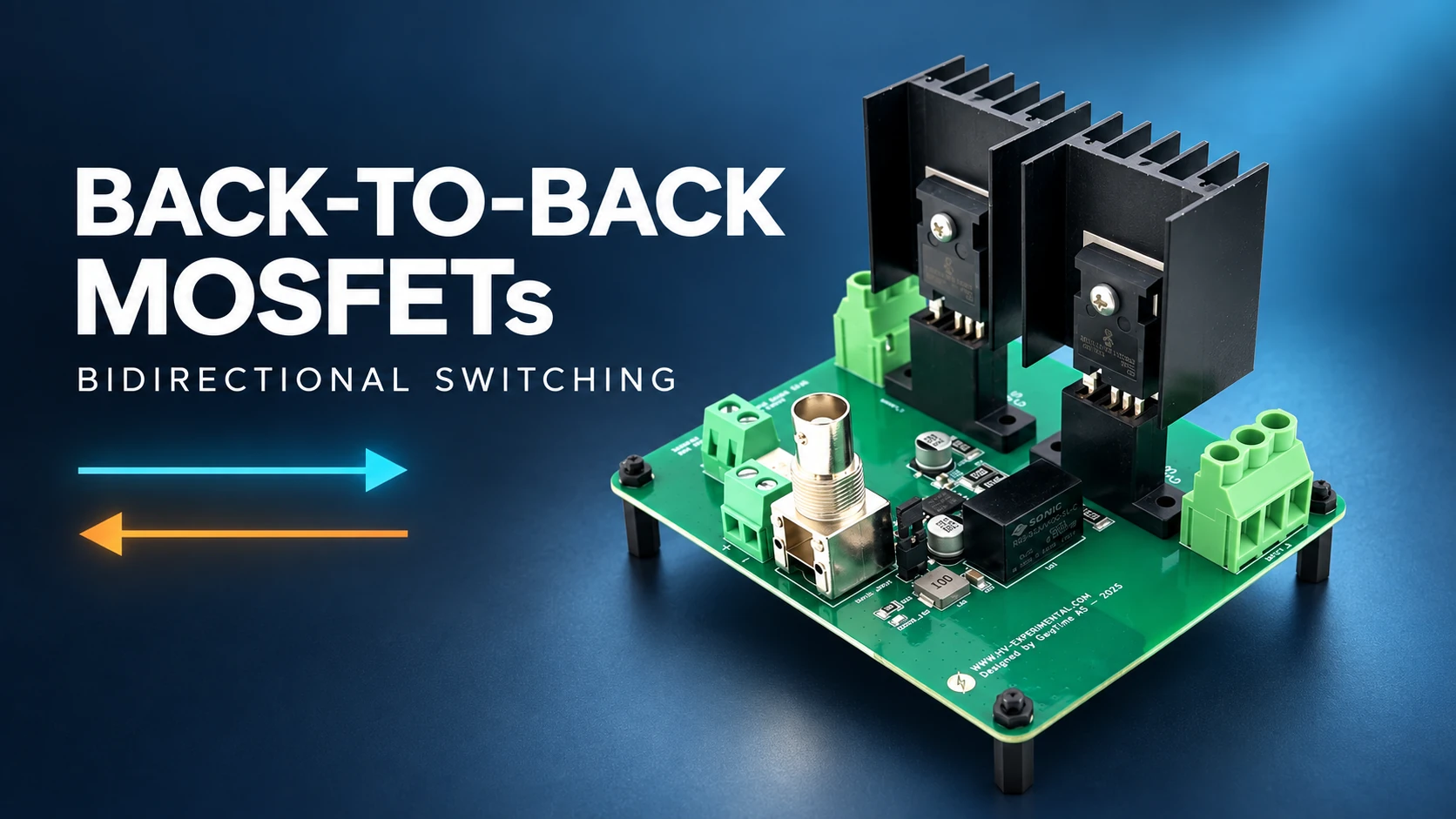
A bidirectional MOSFET switch can be built from two back-to-back MOSFETs to conduct current in either direction when on and block either voltage polarity when off. This makes it useful for AC switching, reverse-current blocking and circuits where the voltage across a disconnected load can change polarity.
The reason for using two devices is the MOSFET's body diode. A single MOSFET can already conduct current in both directions through its channel when correctly driven on. The difficulty is stopping current in both directions when it is off.
This guide explains how the back-to-back configuration solves that problem, the difference between common-source and common-drain connections, and what to check when choosing a high-voltage MOSFET switch board. The diagrams show conventional enhancement-mode N-channel power MOSFETs with their bodies connected to their sources.
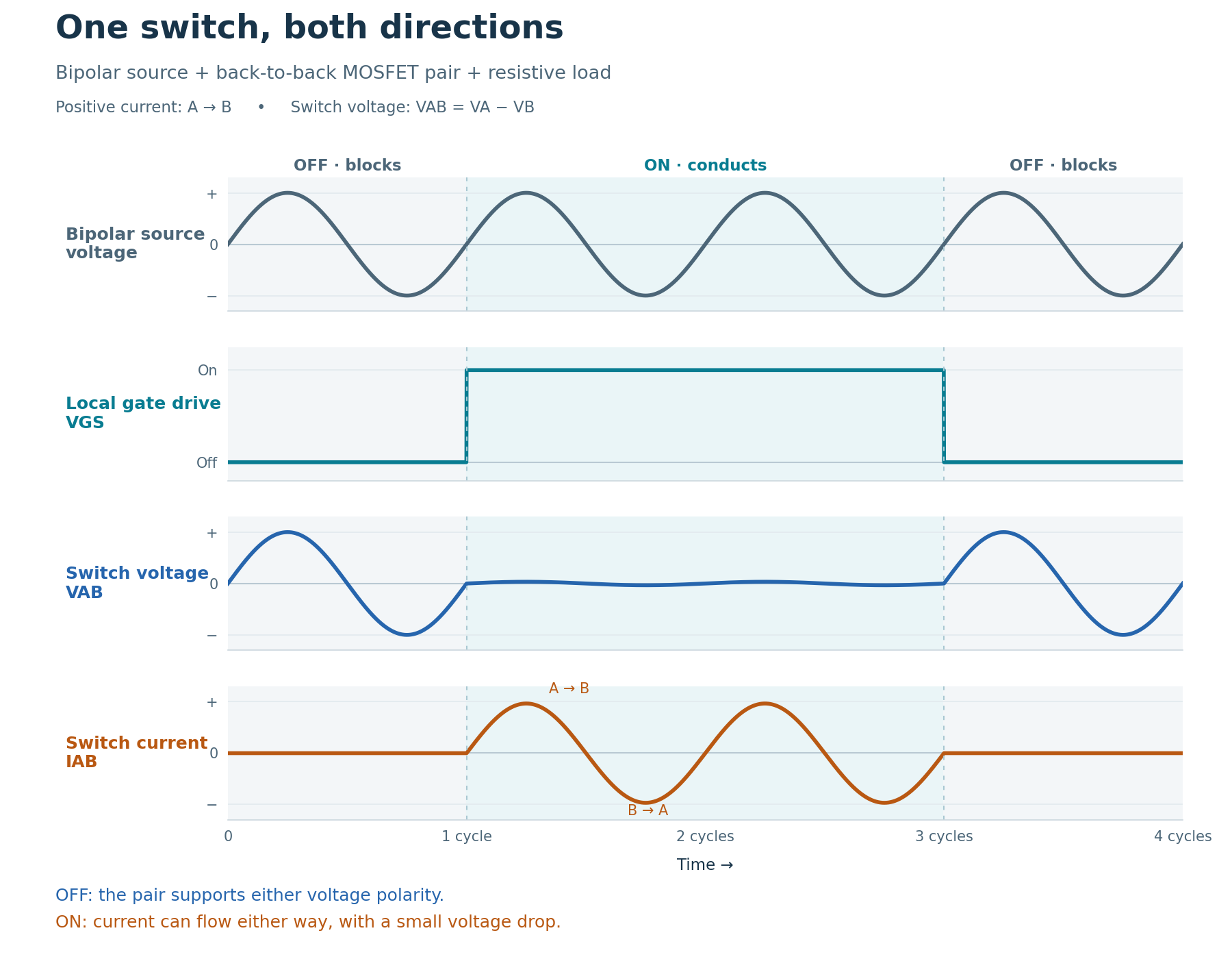
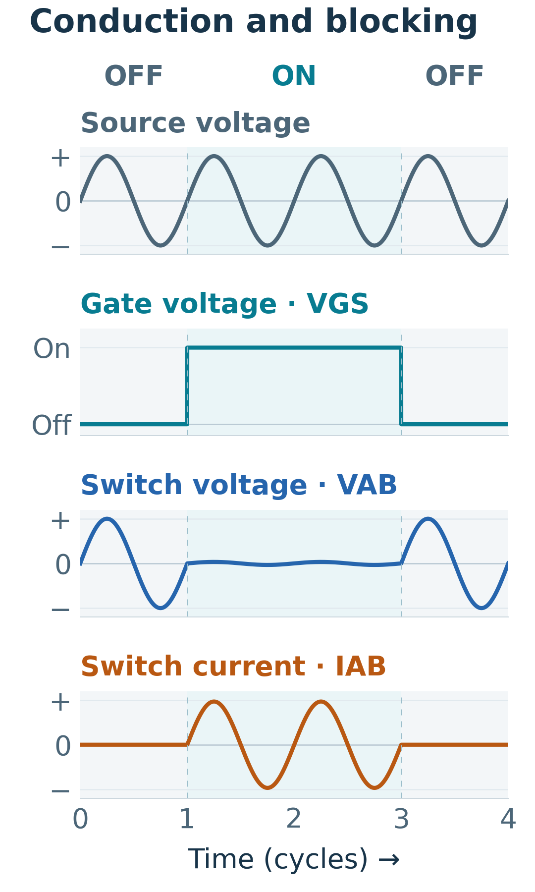
Select any diagram or waveform for a closer look. The drawn waveforms are simplified illustrations; the LC resonant-load example includes real oscilloscope captures. Actual shapes and timings depend on the devices and circuit.
In this guide: The body diode · How the pair works · Gate drive · When to use it · Choosing a board · Common questions
Why a single MOSFET cannot block current both ways
An N-channel power MOSFET has three electrical functions to keep in mind: the controlled channel between drain and source, the gate that controls that channel, and the intrinsic body diode. The diode's anode is at the source and its cathode is at the drain. It therefore allows conventional diode current from source to drain when sufficiently forward biased.
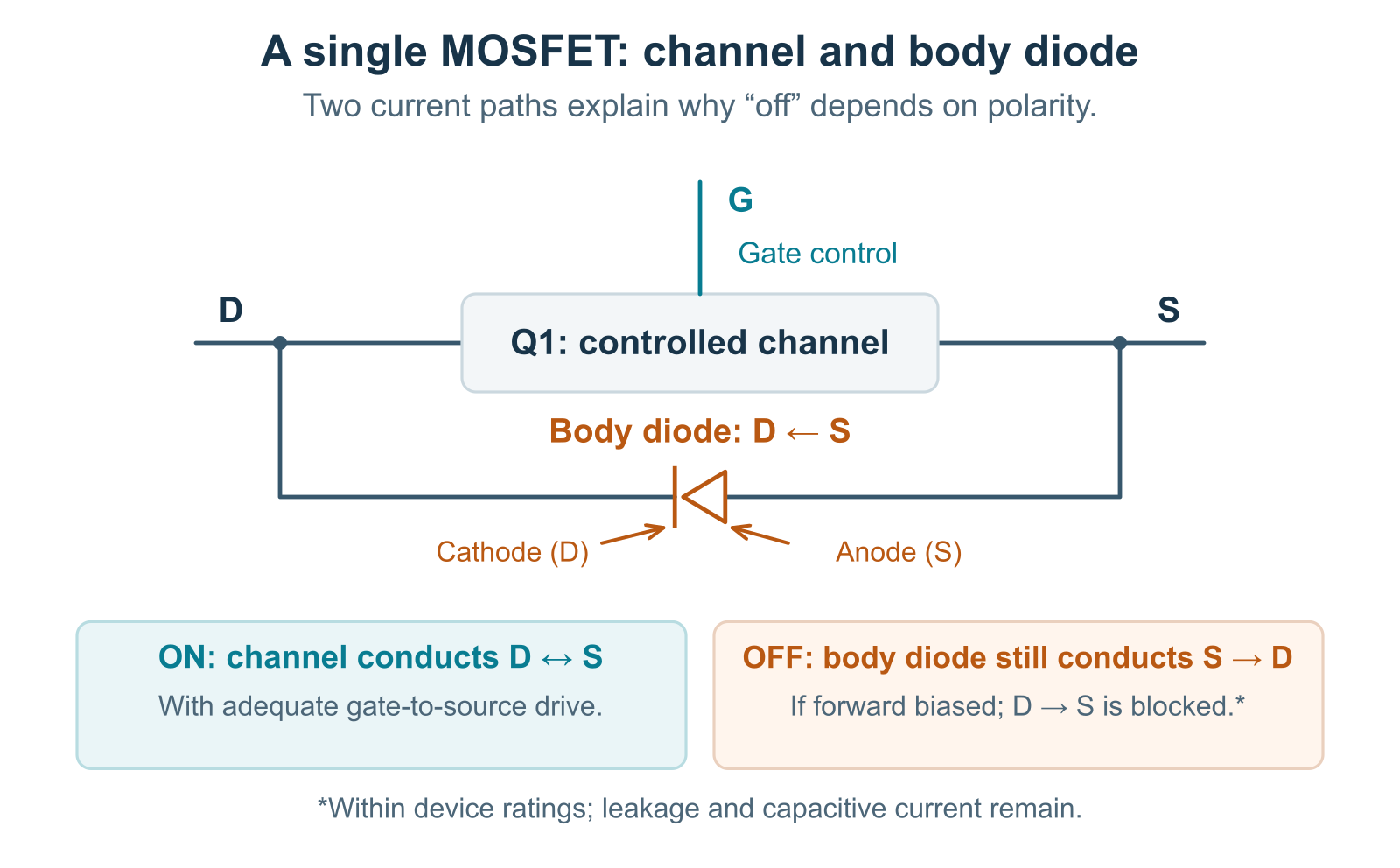
With adequate gate-to-source voltage, the channel behaves approximately like a small resistance and can carry current in either direction. With the gate off, it can block a positive drain-to-source voltage within its ratings. Reverse the applied polarity far enough, however, and the body diode conducts.
That is often acceptable in a DC switching circuit designed around that diode path. It is a problem when an off switch must disconnect both halves of an AC waveform or prevent a charged load from feeding energy back towards its supply.
How a back-to-back MOSFET switch works
Connect two MOSFETs in series but orient them in opposite directions. This is called an anti-series or back-to-back connection. Their body diodes then oppose each other, so they cannot provide one continuous forward-conducting diode path between the two external terminals.
Common-source: the two sources are joined
In a common-source circuit, the connection is drain–source–source–drain. The drains become terminals A and B; the sources meet at the centre. Both gates can be controlled by a suitable driver referenced to that shared source node, usually through separate gate resistors.
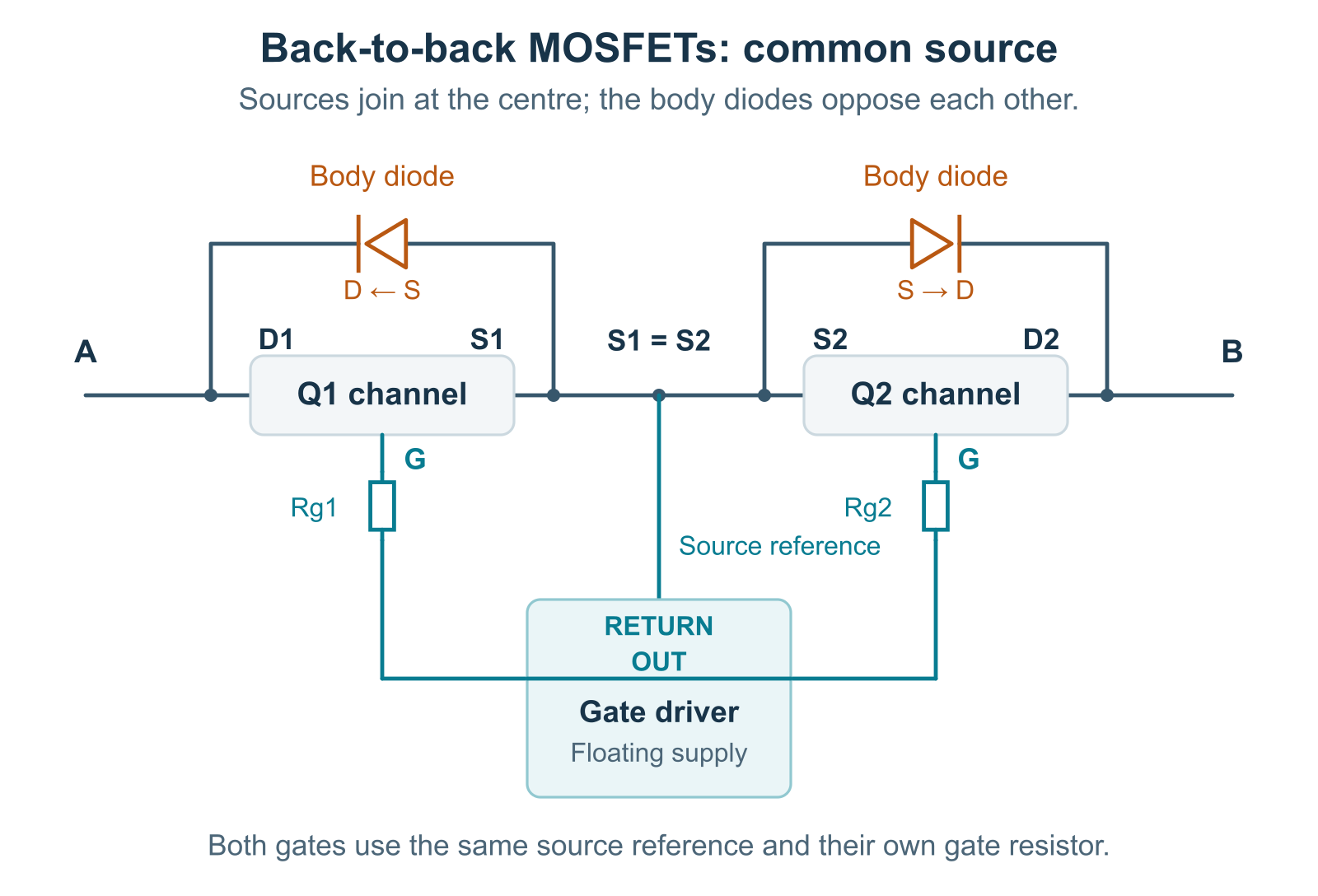
When both MOSFETs are off, Q1 blocks for one terminal polarity and Q2 blocks for the opposite polarity. The other device's body diode can bias the centre node, but the pair still interrupts the through-current path.
When both MOSFETs are properly on, current normally flows through their low-resistance channels rather than through the body diodes. One device carries current from drain to source while the other carries it from source to drain. Using the channels avoids the larger forward-voltage drop of a body diode. A body diode may still conduct during switching or share current if the source-to-drain voltage drop becomes high enough. Current can flow from A to B or from B to A, as determined by the surrounding circuit. The gate-drive signal controls whether the switch is on or off, not which way the current flows.
| Gate state | A positive relative to B | B positive relative to A |
|---|---|---|
| Both off | Q1 blocks the applied voltage | Q2 blocks the applied voltage |
| Both adequately on | Both channels can conduct | Both channels can conduct |
Real devices still have off-state leakage and capacitance. Changing voltage can drive capacitive current even with both gates off. A semiconductor switch therefore does not provide the physical contact gap of a mechanical isolator.
Common-drain: the two drains are joined
The alternative is source–drain–drain–source. The body-diode cathodes meet at the centre and the sources form the external terminals. This arrangement can also provide bidirectional blocking, but the gate-drive references are different: each gate must receive the intended voltage relative to its own source.
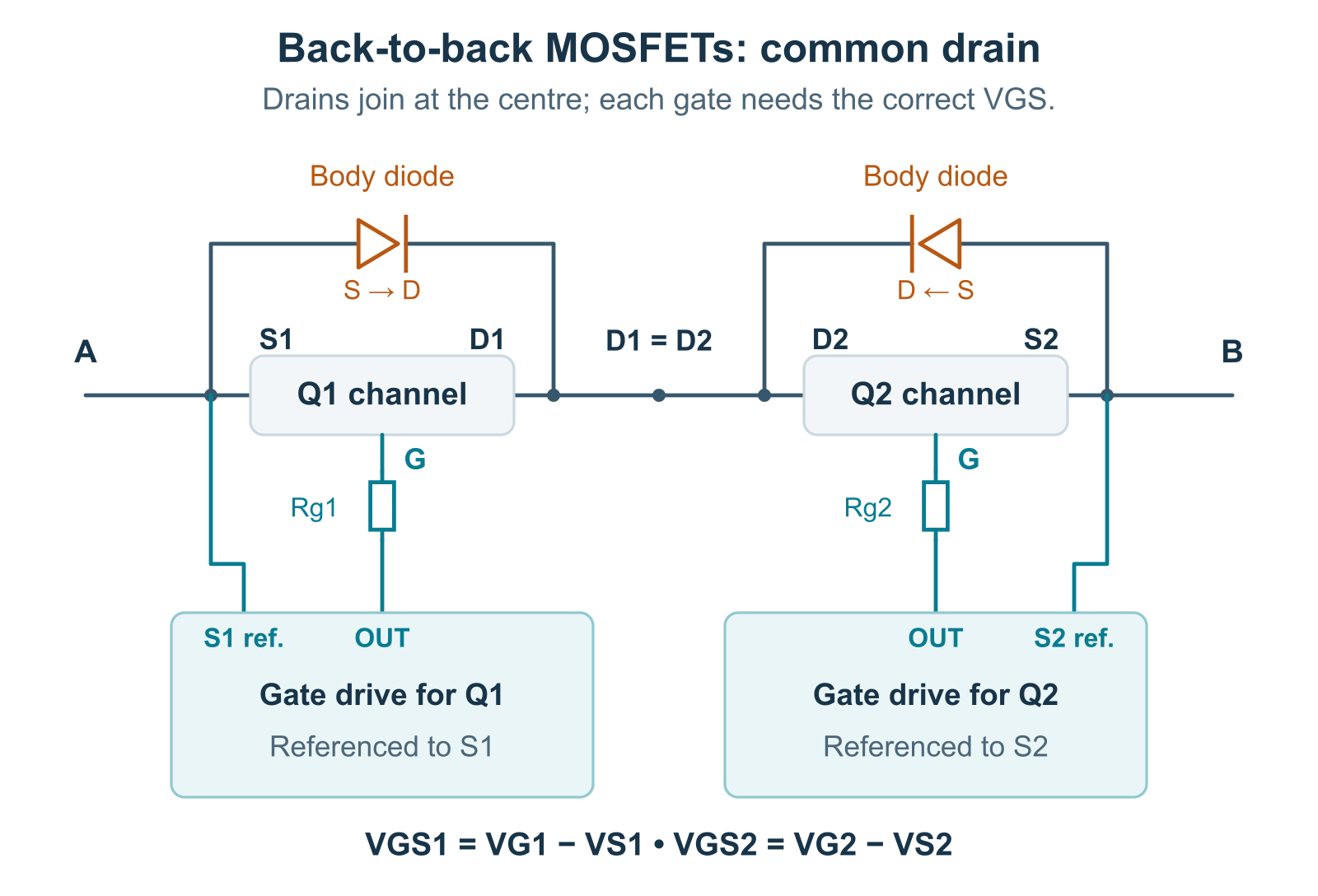
Both configurations appear in Texas Instruments' bidirectional-switch application note. The practical choice depends on the driver, operating voltages and required protection behaviour.
Driving the gates: voltage relative to the source
The relevant control voltage is VGS = VG − VS. A gate that is positive relative to circuit ground is not necessarily positive relative to a floating source. This matters when the switch sits in a high-side position or anywhere in an AC circuit where the source potential moves.
The shared source is not necessarily circuit ground. Depending on the application, the driver needs an appropriate floating supply, isolation or another high-side drive arrangement.
Also distinguish gate threshold voltage from the voltage required for low on-resistance. Threshold marks the onset of conduction at a small test current. Select the drive voltage using the MOSFET's specified RDS(on) conditions and gate-voltage limits. A 3.3 V logic command to a driver board does not imply that the power MOSFET gates operate at 3.3 V. TI's guide to gate-driver fundamentals explains these distinctions.
Gate charge, driver current, gate resistance and layout determine how quickly the pair switches. Both devices add gate charge. At higher frequencies, switching loss, Miller coupling and unwanted gate movement can become as important as conduction loss.
A Kelvin-source connection uses the additional source lead that gives TO-247-4 MOSFETs four pins instead of three. It connects the gate driver to the same source inside the MOSFET, separately from the lead carrying load current. This helps keep fast load-current changes from disturbing the gate voltage.
When do you need a bidirectional MOSFET switch?
Switching AC or a bipolar waveform
If voltage across an off switch can reverse, a single MOSFET's diode may conduct during one polarity. A back-to-back pair provides a way to interrupt both. This is useful in experimental AC circuits, switched resonant networks and other applications requiring a controllable connection without mechanical contacts.
The pair does not generate AC, amplify a signal or create a half-bridge. It controls a connection within a circuit that already supplies the voltage and energy. For sinusoidal voltage, consider the peak value rather than only the RMS value, then allow for transients and the rest of the system's limits.
Disconnecting a load that can feed energy backwards
A capacitor, another power source or an energy-returning load can raise the load-side voltage above the supply-side voltage. Back-to-back MOSFETs can form the disconnect element in a circuit that must prevent this reverse current when disabled.
Where an ordinary MOSFET switch is sufficient
A single-device switch may be the better fit when the off-state voltage has one known polarity and the circuit intentionally accommodates the body diode. It uses one device's on-resistance and gate charge rather than two. The decision is therefore about the required off-state blocking, not simply whether current can reverse while the switch is on.
Real measurements: switching off an LC resonant load
These oscilloscope captures show the voltage across the switch after turn-off. In this test circuit, the LC tank was connected ahead of the switch. CH2 measured the voltage from one switch terminal to the other.
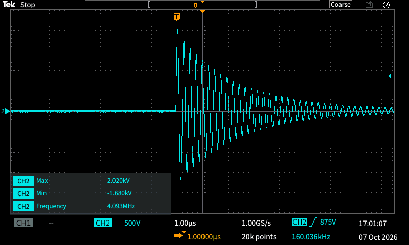
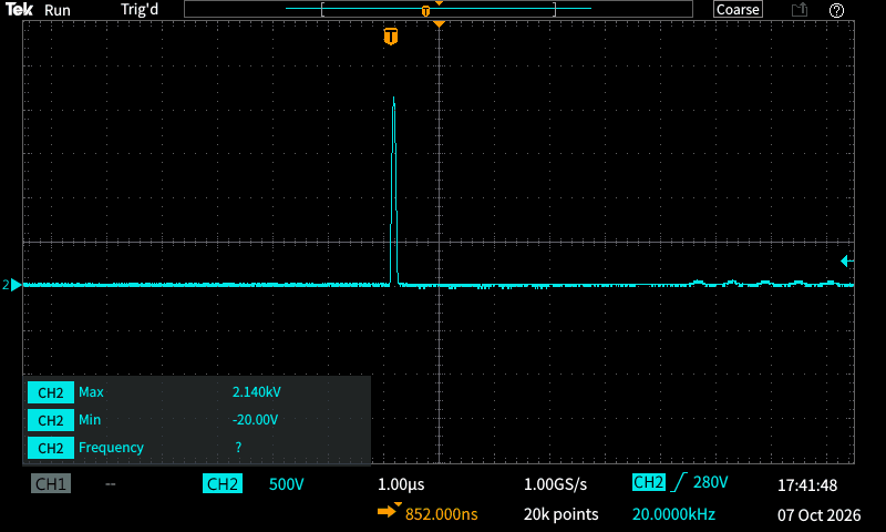
The single-MOSFET trace is consistent with its body diode conducting when the switch voltage reverses, limiting that part of the oscillation. With a back-to-back pair, the opposing body diodes block this path while both channels are off. The ringing voltage across the pair does not mean its channels are still on.
This matters when switching components in an LC resonant circuit. Adding or removing a capacitor or inductor changes the circuit’s tuning. A single MOSFET can leave an unwanted diode path even after its gate is turned off, changing how the circuit resonates. A bidirectional MOSFET switch lets the connection block either voltage polarity when off. The resulting waveform still depends on the circuit’s losses, device capacitances and layout.
Voltage, current and switching limits to check
Two back-to-back MOSFETs do not double the voltage rating
For one voltage polarity, one device can support nearly the full voltage across the pair. Reverse the polarity and the roles swap. Each device must therefore withstand the relevant terminal voltage and overshoot. This differs from a series stack engineered to share voltage across several stages.
Both on-resistances contribute to heating
A first estimate of total conduction loss is:
Pconduction ≈ IRMS2 × [RDS(on),1 + RDS(on),2]
For example, if each device has 0.10 Ω on-resistance at the chosen operating condition and the current is 2 A RMS, the pair dissipates approximately 0.8 W from conduction alone. Use resistance at the expected temperature and drive voltage, then account separately for switching losses and cooling.
The load determines what happens at turn-off
Inductive current needs somewhere to go when the switch opens. Load inductance and wiring inductance can produce voltage overshoot; a suitable clamp, snubber or commutation path must be designed for the circuit. A MOSFET's nominal current rating alone does not establish that it can safely interrupt the load. Check transient energy, safe operating area and thermal limits. Infineon's bidirectional-switch analysis examines these stresses.
Check the MOSFET's avalanche rating too. A turn-off spike can push the device into drain-to-source breakdown, where it absorbs energy as heat. Too much can damage it. The single-pulse energy rating EAS applies only under the stated current, pulse and starting-temperature conditions. This does not guarantee repeated avalanche is safe. Check the manufacturer's repetitive-avalanche limits for current, temperature and repetition rate. Do not assume the back-to-back devices share the energy equally. A suitable clamp or freewheel path should normally handle the inductive energy.
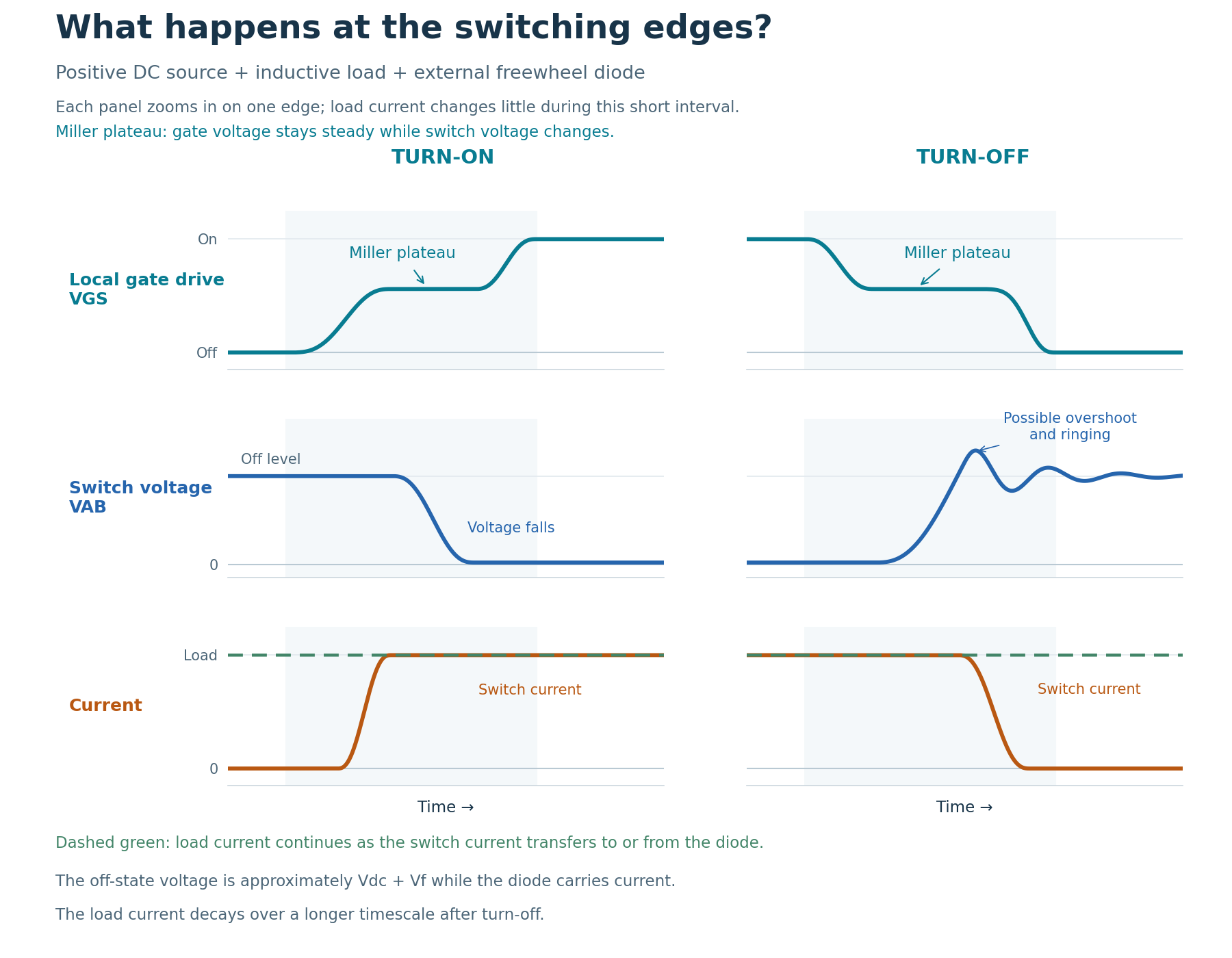
The Miller plateau: a pause in gate voltage
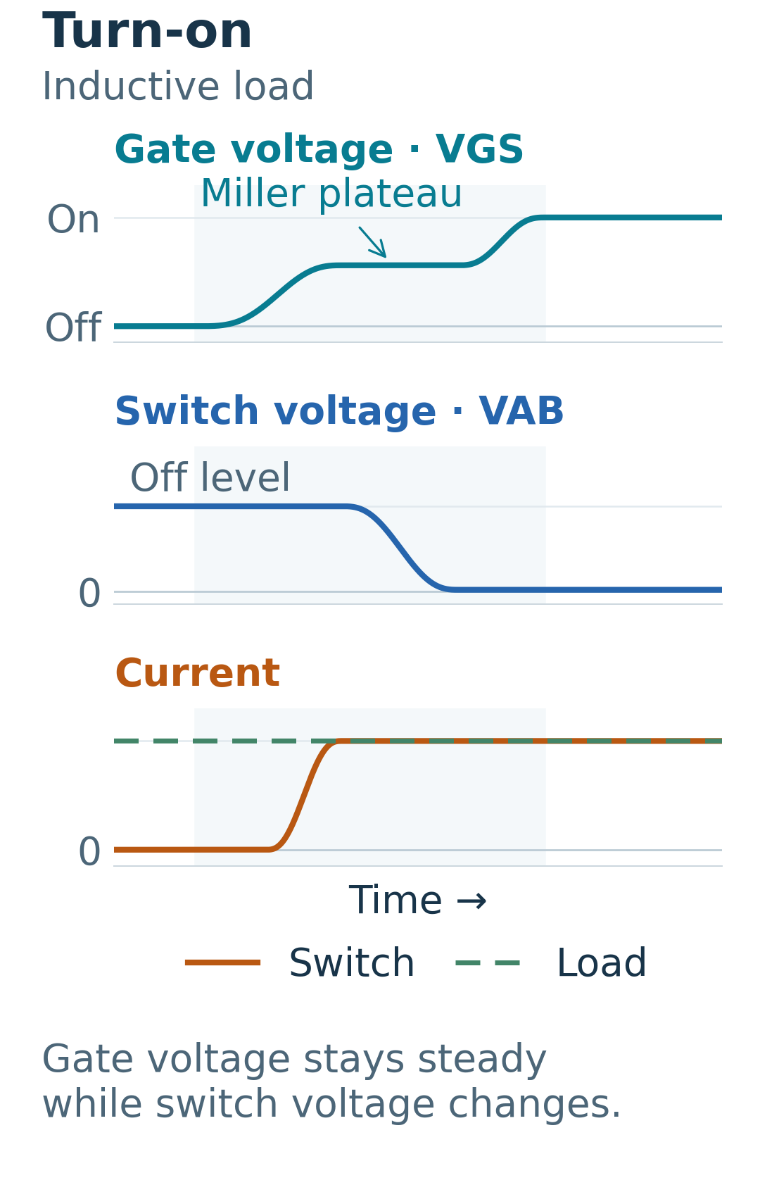
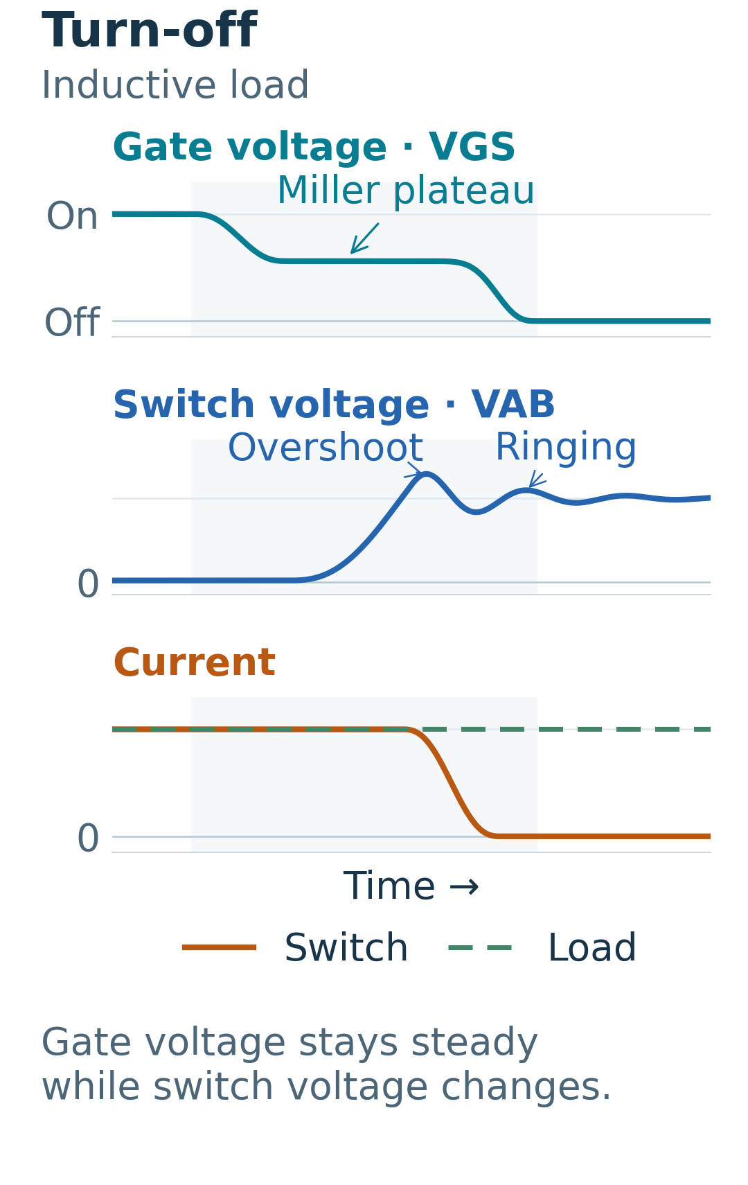
The nearly flat part of the gate-voltage trace in the switching example below is called the Miller plateau. During this interval, the gate driver moves charge through the gate-to-drain capacitance. The gate-to-source voltage changes very little while the drain-to-source voltage changes rapidly. In this positive-DC inductive-load example, the voltage across the MOSFET pair falls at turn-on and rises at turn-off.
The time needed to move that charge determines how long the plateau lasts. This depends on the amount of charge involved, called the Miller charge, and how much current the driver can deliver to or draw from the gates. A weaker gate drive or larger gate resistance generally lengthens the plateau and slows the voltage transition. Once the transition is complete, the gate voltage continues towards its final on or off level.
When checking a real circuit on an oscilloscope, use appropriately rated differential or isolated measurement equipment for floating nodes. Never connect an ordinary earth-referenced oscilloscope ground clip to a floating high-voltage source node. The power terminals can still be at a dangerous voltage when the switch is off, even if the gate driver is isolated.
Choosing a high-voltage MOSFET switch board
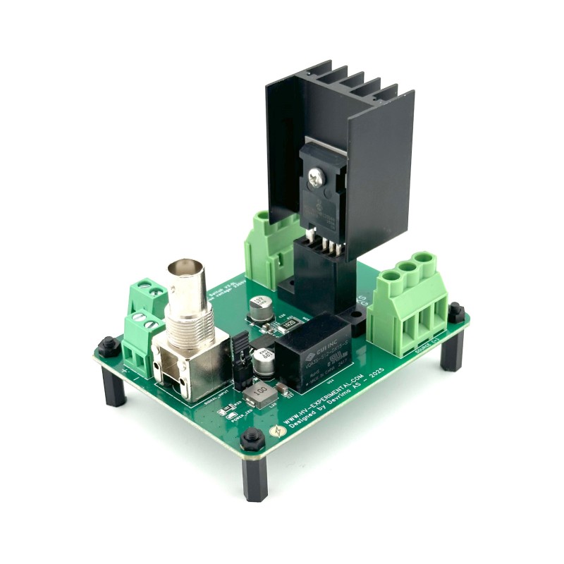
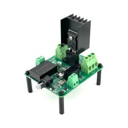
Start with the blocking behaviour, then choose the package, fitted MOSFETs and driver. The HVE MOSFET switch board range includes standard, bidirectional and optical stackable designs for these different requirements.
| Your requirement | Relevant board | Why choose it? |
|---|---|---|
| One-polarity off-state blocking with a TO-247-4 device | MOSFET Switch Board, TO-247-4 | Single socketed device and dedicated Kelvin-source gate reference. |
| Two-polarity blocking and bidirectional conduction | Bidirectional MOSFET Switch Board, TO-247-4 | Back-to-back socketed devices with Kelvin-source connections. |
| A bidirectional switch using the three-lead TO-247 package | Bidirectional MOSFET Switch Board, TO-247 | Three-lead TO-247 option with a common-source topology. |
| Voltage sharing across multiple series stages | Stackable MOSFET Switch Board, Optical Input | A separate architecture for coordinated series switching; it does not inherently provide back-to-back blocking. |
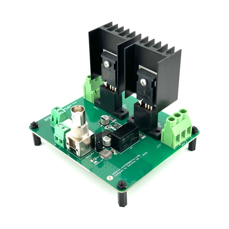
The HVE TO-247 and TO-247-4 bidirectional boards both use a 12 V supply and accept a 0–3.3 V or 0–5 V square-wave control signal through BNC. The TO-247 version specifies −4/+15 V gate-drive rails; the TO-247-4 version specifies −5/+18 V. Check those rails against the installed MOSFET's datasheet. Package fit alone does not establish electrical compatibility.
The TO-247-4 board's Kelvin-source arrangement is particularly relevant when fast current changes would otherwise disturb the gate reference. Its published switching figures still depend on the selected MOSFETs, load and operating conditions; they are not a guarantee at every combination of voltage, current and frequency.
Finally, keep drain-source voltage rating separate from control-to-switch isolation. A fitted MOSFET's voltage rating, the driver's isolation limit and the complete circuit's clearances, transients and thermal limits are different constraints. Check all of them before choosing the operating voltage.
Compare HVE MOSFET switch boards to select the topology first, then review the individual board's device options, gate drive and operating limits.
Common questions about back-to-back MOSFETs
Can a MOSFET conduct current in both directions?
Yes. An adequately enhanced MOSFET channel can conduct either way. A conventional single N-channel power MOSFET cannot provide two-polarity off-state blocking because of its source-to-drain body diode.
Can I connect the gates together?
A common-source pair can use one suitable driver referenced to the shared source, with individual gate resistors where required. A common-drain circuit needs a driver arrangement that maintains the intended voltage between each gate and its own source. Do not assume the two arrangements are interchangeable.
Is a back-to-back MOSFET pair the same as a half-bridge?
No. A half-bridge uses a high-side and low-side device around a switching node, with coordinated timing to avoid a supply short. A back-to-back pair acts as one series connection that can block either polarity. The purpose and gate-control requirements differ.
Does a bidirectional MOSFET switch provide galvanic isolation?
No. Turning the switch off blocks the main current flow between its power terminals, but does not create an insulating gap. An isolated gate driver can separate the control electronics from the high-voltage circuit. It does not provide isolation between the switch's two power terminals.
Can two 1,200 V MOSFETs back-to-back block 2,400 V?
No. In an anti-series pair, each MOSFET must be able to withstand the relevant voltage across the switch, including transients. A voltage-sharing series stack is a different design problem.
Technical references
- Texas Instruments: Achieve Bidirectional Control and Protection Through Back-to-Back Connected eFuse Devices — bidirectional-switch behaviour and common-source/common-drain configurations.
- Texas Instruments: Fundamentals of MOSFET and IGBT Gate Driver Circuits — gate drive, the Miller plateau and switching behaviour.
- Infineon: MOSFET Bidirectional Switch (BDS) Analysis in Battery Management Systems — transient stress and safe operating area.
- Infineon: Power MOSFET Avalanche Design Guidelines — single-pulse ratings and repeated avalanche events.

No comments yet. Be the first to start the conversation.